 |
Os motores de busca de Datasheet de Componentes eletrônicos |
|
|
Os motores de busca de Datasheet de Componentes eletrônicos |
|
The question interval is too short.
Please try again in a few seconds.

Hello, Please ask a question about LTC1293 Datasheet
# Example questions:
➢ What potential issue arises if the analog or reference input voltage exceeds the supply voltage (vcc) by more than 50mv, and what is the recommended minimum supply voltage to ensure a 0v to 5v input range?
➢ What is the typical supply voltage (vcc) used for the specifications outlined in the document?
➢ How does decreasing the clock frequency affect the error (specifically, the change in code transition) and what does the graph represent regarding minimum clock frequency?
| Part No. | LTC1293 |
| Manufacturer | LINER |
| Size | 494 Kbytes |
| Pages | 28 pages |
| Description | Single Chip 12-Bit Data Acquisition System |

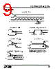
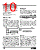
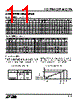
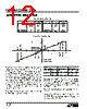
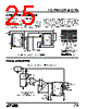
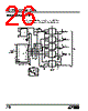
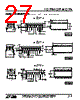
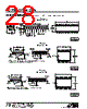

1. Overview
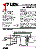
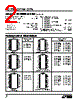
The document is a section of the datasheet for the LTC1293/4/6 Analog-to-Digital Converters (ADCs). These are mixed-signal, 12-bit ADCs with a built-in EEPROM for calibration data. They are designed for data acquisition systems and other applications requiring high resolution and flexibility.
2. Key Specifications (Selected)
️· Resolution: 12 bits
️· Input Voltage Range: 0V to 5V (unipolar); bipolar input range available.
️· Conversion Speed: The data sheet does not provide conversion speed data, however the note on minimum clock rate is pertinent.
️· Minimum Clock Rate (for 0.1 LSB Error): This is dependent on the application - the datasheet refers to a graph.
️· Supply Voltage (Vcc): 5V (typical operating voltage)
️· Reference Voltages: VREF + = 5V, V REF – = 0V (unipolar); –5V (bipolar)
️· EEPROM: Built-in for calibration data.
3. Important Notes and Clarifications
️· Note 1 (Absolute Maximum Ratings): These are maximum values; exceeding them can damage the ADC.
️· Note 2 (Reference to Ground): All voltage values are referenced to a common ground (DGND, AGND, REF [–] tied together).
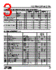
️· Note 3 (Operating Conditions): All specifications are given at Vcc = 5V, VREF + = 5V, VREF – = 0V, and a clock frequency of 1 MHz, unless otherwise stated. "G" means specifications are guaranteed over the full operating temperature range.
️· Note 4 (Bipolar Mode): In bipolar mode, 1 LSB is the bipolar input span (2VREF) divided by 4096. Example: with VREF = 5V, 1 LSB (bipolar) = 2.44mV.
️· Note 5 (Linearity Error): Linearity error is specified between the actual end points of the A/D transfer curve and deviation is measured from the center of the quantization band.
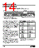
️· Note 6 (Minimum Clock Rate and Error): The datasheet includes a graph and note, explaining that, as the clock frequency is decreased from 1MHz, the “minimum clock rate (∆ error ≤ 0.1LSB)” represents the frequency at which a 0.1LSB shift in any code transition from its 1MHz value is first detected.
️· Note 7 (Input Voltage Limits): Due to internal diodes, caution is needed with low Vcc values (e.g., 4.5V) to prevent diode conduction, which can cause errors when inputs are near full scale. An absolute 0V to 5V input voltage range requires a minimum supply voltage of 4.950V to account for tolerances, temperature and loading.
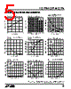
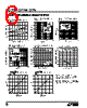
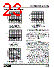
4. Descriptions of Graphs (Since I can't show the actual graphs):
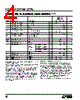
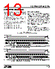
️· Supply Current vs. Supply Voltage: This graph shows the current drawn by the ADC as the supply voltage increases. It's used to determine power consumption.
️· Supply Current vs. Temperature: This graph shows how the current consumption changes with temperature.
️· Unadjusted Offset Voltage vs. Reference Voltage: This shows the offset voltage as a function of the reference voltage.
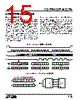
️· Change in Linearity vs. Reference Voltage: This graph plots the change in linearity error with changes in the reference voltage.
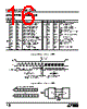
️· Change in Gain vs. Reference Voltage: This graph shows how gain error changes with changes in the reference voltage.
️· Change in Offset vs. Temperature: This graph indicates how offset voltage changes with temperature.
️· Change in Linearity vs. Temperature: This graph displays the change in linearity error as a function of temperature.
️· Change in Gain vs. Temperature: This graph depicts how gain error varies with temperature.
5. Summary
The LTC1293/4/6 ADCs are high-resolution converters with built-in calibration. Understanding the limitations with input voltage ranges, clock frequency, and the impact of temperature and reference voltage is vital for successful application. The datasheet emphasizes the importance of careful design and consideration of these factors to achieve desired performance.
1. Overview
The document is a section of the datasheet for the LTC1293/4/6 Analog-to-Digital Converters (ADCs). These are mixed-signal, 12-bit ADCs with a built-in EEPROM for calibration data. They are designed for data acquisition systems and other applications requiring high resolution and flexibility.
2. Key Specifications (Selected)
️· Resolution: 12 bits
️· Input Voltage Range: 0V to 5V (unipolar); bipolar input range available.
️· Conversion Speed: The data sheet does not provide conversion speed data, however the note on minimum clock rate is pertinent.
️· Minimum Clock Rate (for 0.1 LSB Error): This is dependent on the application - the datasheet refers to a graph.
️· Supply Voltage (Vcc): 5V (typical operating voltage)
️· Reference Voltages: VREF + = 5V, V REF – = 0V (unipolar); –5V (bipolar)
️· EEPROM: Built-in for calibration data.
3. Important Notes and Clarifications
️· Note 1 (Absolute Maximum Ratings): These are maximum values; exceeding them can damage the ADC.
️· Note 2 (Reference to Ground): All voltage values are referenced to a common ground (DGND, AGND, REF [–] tied together).
️· Note 3 (Operating Conditions): All specifications are given at Vcc = 5V, VREF + = 5V, VREF – = 0V, and a clock frequency of 1 MHz, unless otherwise stated. "G" means specifications are guaranteed over the full operating temperature range.
️· Note 4 (Bipolar Mode): In bipolar mode, 1 LSB is the bipolar input span (2VREF) divided by 4096. Example: with VREF = 5V, 1 LSB (bipolar) = 2.44mV.
️· Note 5 (Linearity Error): Linearity error is specified between the actual end points of the A/D transfer curve and deviation is measured from the center of the quantization band.
️· Note 6 (Minimum Clock Rate and Error): The datasheet includes a graph and note, explaining that, as the clock frequency is decreased from 1MHz, the “minimum clock rate (∆ error ≤ 0.1LSB)” represents the frequency at which a 0.1LSB shift in any code transition from its 1MHz value is first detected.
️· Note 7 (Input Voltage Limits): Due to internal diodes, caution is needed with low Vcc values (e.g., 4.5V) to prevent diode conduction, which can cause errors when inputs are near full scale. An absolute 0V to 5V input voltage range requires a minimum supply voltage of 4.950V to account for tolerances, temperature and loading.
4. Descriptions of Graphs (Since I can't show the actual graphs):
️· Supply Current vs. Supply Voltage: This graph shows the current drawn by the ADC as the supply voltage increases. It's used to determine power consumption.
️· Supply Current vs. Temperature: This graph shows how the current consumption changes with temperature.
️· Unadjusted Offset Voltage vs. Reference Voltage: This shows the offset voltage as a function of the reference voltage.
️· Change in Linearity vs. Reference Voltage: This graph plots the change in linearity error with changes in the reference voltage.
️· Change in Gain vs. Reference Voltage: This graph shows how gain error changes with changes in the reference voltage.
️· Change in Offset vs. Temperature: This graph indicates how offset voltage changes with temperature.
️· Change in Linearity vs. Temperature: This graph displays the change in linearity error as a function of temperature.
️· Change in Gain vs. Temperature: This graph depicts how gain error varies with temperature.
5. Summary
The LTC1293/4/6 ADCs are high-resolution converters with built-in calibration. Understanding the limitations with input voltage ranges, clock frequency, and the impact of temperature and reference voltage is vital for successful application. The datasheet emphasizes the importance of careful design and consideration of these factors to achieve desired performance.
| Part No. | LTC1293 |
| Manufacturer | LINER |
| Size | 494 Kbytes |
| Pages | 28 pages |
| Description | Single Chip 12-Bit Data Acquisition System |
| ALLDATASHEET é útil para você? [ DONATE ] |
Sobre Alldatasheet | Publicidade | Contato conosco | Privacy Policy | Link para a ficha técnica | roca de Link | Lista de Fabricantes All Rights Reserved©Alldatasheet.com |
| Russian : Alldatasheetru.com | Korean : Alldatasheet.co.kr | Spanish : Alldatasheet.es | French : Alldatasheet.fr | Italian : Alldatasheetit.com Portuguese : Alldatasheetpt.com | Polish : Alldatasheet.pl | Vietnamese : Alldatasheet.vn Indian : Alldatasheet.in | Mexican : Alldatasheet.com.mx | British : Alldatasheet.co.uk | New Zealand : Alldatasheet.co.nz |
|
Family Site : ic2ic.com |
icmetro.com |
 Portuguese ▼
  English
 Chinese
 German
 Japanese
 Russian
 Korean
 Spanish
 French
 Italian
 Polish
 Vietnamese
 Indian
 Mexican
 British
 New Zealand