 |
Os motores de busca de Datasheet de Componentes eletrônicos |
|
|
Os motores de busca de Datasheet de Componentes eletrônicos |
|
The question interval is too short.
Please try again in a few seconds.

Hello, Please ask a question about LT1368_15 Datasheet
# Example questions:
➢ Compare the typical short-circuit current (i_sc) values specified for a temperature range of 0°c to 70°c versus at 25°c.
➢ At 25°c, what is the range of typical large-signal voltage gain (a_vol) for the lt1366/lt1367/lt1368/lt1369 amplifiers?
➢ What is the typical supply current for the lt1366/lt1367/lt1368/lt1369 amplifiers when v_s = 3v?
| Part No. | LT1368_15 |
| Manufacturer | LINER |
| Size | 392 Kbytes |
| Pages | 20 pages |
| Description | Dual and Quad Precision Rail-to-Rail Input and Output Op Amps |


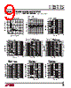


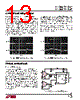


Important Notes & Issues with the Text:
️· Redundancy and Layout Variations: The text is presented almost identically in both blocks, but with some variations in table layout.
️· "l" Notation: The "l" notation appears to indicate specifications that apply over a temperature range of 0°C < T<sub>A</sub> < 70°C.
️· Conflicting Data: There are subtle discrepancies between the two tables. This is a common problem with data extracted from technical documents that might be early drafts or have editorial inconsistencies.
️· Unclear Gain Voltage: Some tables use "VO = 50mV to 2.8V" others use "VO = 50mV to 2.8V, RL = 10k". I'm making the assumption that the second is the more accurate definition (with an output voltage from 50mV to 2.8V with a 10k Ohm load).
Organized Electrical Characteristics (Combining Data & Noting Differences):
I'm presenting a combined table. I've noted where the tables differ. I will split the information based on LT1366/LT1368 and LT1367/LT1369.
LT1366/LT1368 Characteristics:
| Parameter | Conditions | Value (Temperature Range: 0°C < T<sub>A</sub> < 70°C) | Value (3V, 0V, 1.5V, 1.5V) | Notes |
|---|---|---|---|---|
| Input Offset Voltage (VOS) | VCM = VCC, VCM = VEE | 200 µV | 200 µV | |
| 575 µV | ||||
| Input Offset Voltage Drift (VOS TC) | 2 µV/°C | |||
| 6 µV/°C | ||||
| Input Bias Current (IB) | VCM = VCC | 0 nA | ||
| -45 nA | ||||
| 15 nA | ||||
| -10 nA | ||||
| 45 nA | ||||
| 0 nA | ||||
| Input Offset Current (IOS) | VCM = VCC | 2 nA | ||
| 1 nA | ||||
| 15 nA | ||||
| 15 nA | ||||
| Large-Signal Voltage Gain (AVOL) | VO = 50mV to 2.8V, RL = 10k | 250 | ||
| 1500 | ||||
| Common Mode Rejection Ratio (CMRR) | VCM = VEE to VCC | 76 dB | ||
| 70 dB | ||||
| 83 dB | ||||
| 83 dB | ||||
| Output Voltage Swing Low (VOL) | No Load, ISINK = 0.5mA | 9 mV | ||
| 45 mV | ||||
| 120 mV | ||||
| 14 mV | ||||
| 80 mV | ||||
| 230 mV | ||||
| Output Voltage Swing High (VOH) | No Load, ISOURCE = 0.5mA | VCC – 0.014 V | ||
| VCC – 0.110 V | ||||
| VCC – 0.250 V | ||||
| VCC – 0.005 V | ||||
| VCC – 0.055 V | ||||
| VCC – 0.180 V | ||||
| Short-Circuit Current (ISC) | ±10 mA | |||
| Supply Current per Amplifier (IS) | 375 µA | |||
| 520 µA |
| Parameter | Conditions | Value (Temperature Range: 0°C < T<sub>A</sub> < 70°C) | Value (3V, 0V, 1.5V, 1.5V) | Notes |
|---|---|---|---|---|
| Input Offset Voltage (VOS) | VCM = VCC, VCM = VEE | 200 µV | 200 µV | |
| 950 µV | ||||
| Input Offset Voltage Drift (VOS TC) | 2 µV/°C | |||
| 6 µV/°C | ||||
| Input Bias Current (IB) | VCM = VCC | 0 nA | ||
| -35 nA | ||||
| 10 nA | ||||
| -10 nA | ||||
| 35 nA | ||||
| 0 nA | ||||
| Input Offset Current (IOS) | VCM = VCC | 2 nA | ||
| 0.3 nA | ||||
| 12 nA | ||||
| 12 nA | ||||
| Large-Signal Voltage Gain (AVOL) | VO = 50mV to 2.8V, RL = 10k | 150 | ||
| 1500 | ||||
| Common Mode Rejection Ratio (CMRR) | VCM = VEE to VCC | 72 dB | ||
| 66 dB | ||||
| 83 dB | ||||
| 83 dB | ||||
| Output Voltage Swing Low (VOL) | No Load, ISINK = 0.5mA | 6 mV | ||
| 40 mV | ||||
| 110 mV | ||||
| 12 mV | ||||
| 70 mV | ||||
| 200 mV | ||||
| Output Voltage Swing High (VOH) | No Load, ISOURCE = 0.5mA | VCC – 0.012 V | ||
| VCC – 0.100 V | ||||
| VCC – 0.250 V | ||||
| VCC – 0.004 V | ||||
| VCC – 0.050 V | ||||
| VCC – 0.150 V | ||||
| Short-Circuit Current (ISC) | ±10 mA | |||
| Supply Current per Amplifier (IS) | 330 µA | |||
| 500 µA |
Important Notes & Issues with the Text:
️· Redundancy and Layout Variations: The text is presented almost identically in both blocks, but with some variations in table layout.
️· "l" Notation: The "l" notation appears to indicate specifications that apply over a temperature range of 0°C < T<sub>A</sub> < 70°C.
️· Conflicting Data: There are subtle discrepancies between the two tables. This is a common problem with data extracted from technical documents that might be early drafts or have editorial inconsistencies.
️· Unclear Gain Voltage: Some tables use "VO = 50mV to 2.8V" others use "VO = 50mV to 2.8V, RL = 10k". I'm making the assumption that the second is the more accurate definition (with an output voltage from 50mV to 2.8V with a 10k Ohm load).
Organized Electrical Characteristics (Combining Data & Noting Differences):
I'm presenting a combined table. I've noted where the tables differ. I will split the information based on LT1366/LT1368 and LT1367/LT1369.
LT1366/LT1368 Characteristics:
| Parameter | Conditions | Value (Temperature Range: 0°C < T<sub>A</sub> < 70°C) | Value (3V, 0V, 1.5V, 1.5V) | Notes |
|---|---|---|---|---|
| Input Offset Voltage (VOS) | VCM = VCC, VCM = VEE | 200 µV | 200 µV | |
| 575 µV | ||||
| Input Offset Voltage Drift (VOS TC) | 2 µV/°C | |||
| 6 µV/°C | ||||
| Input Bias Current (IB) | VCM = VCC | 0 nA | ||
| -45 nA | ||||
| 15 nA | ||||
| -10 nA | ||||
| 45 nA | ||||
| 0 nA | ||||
| Input Offset Current (IOS) | VCM = VCC | 2 nA | ||
| 1 nA | ||||
| 15 nA | ||||
| 15 nA | ||||
| Large-Signal Voltage Gain (AVOL) | VO = 50mV to 2.8V, RL = 10k | 250 | ||
| 1500 | ||||
| Common Mode Rejection Ratio (CMRR) | VCM = VEE to VCC | 76 dB | ||
| 70 dB | ||||
| 83 dB | ||||
| 83 dB | ||||
| Output Voltage Swing Low (VOL) | No Load, ISINK = 0.5mA | 9 mV | ||
| 45 mV | ||||
| 120 mV | ||||
| 14 mV | ||||
| 80 mV | ||||
| 230 mV | ||||
| Output Voltage Swing High (VOH) | No Load, ISOURCE = 0.5mA | VCC – 0.014 V | ||
| VCC – 0.110 V | ||||
| VCC – 0.250 V | ||||
| VCC – 0.005 V | ||||
| VCC – 0.055 V | ||||
| VCC – 0.180 V | ||||
| Short-Circuit Current (ISC) | ±10 mA | |||
| Supply Current per Amplifier (IS) | 375 µA | |||
| 520 µA |
| Parameter | Conditions | Value (Temperature Range: 0°C < T<sub>A</sub> < 70°C) | Value (3V, 0V, 1.5V, 1.5V) | Notes |
|---|---|---|---|---|
| Input Offset Voltage (VOS) | VCM = VCC, VCM = VEE | 200 µV | 200 µV | |
| 950 µV | ||||
| Input Offset Voltage Drift (VOS TC) | 2 µV/°C | |||
| 6 µV/°C | ||||
| Input Bias Current (IB) | VCM = VCC | 0 nA | ||
| -35 nA | ||||
| 10 nA | ||||
| -10 nA | ||||
| 35 nA | ||||
| 0 nA | ||||
| Input Offset Current (IOS) | VCM = VCC | 2 nA | ||
| 0.3 nA | ||||
| 12 nA | ||||
| 12 nA | ||||
| Large-Signal Voltage Gain (AVOL) | VO = 50mV to 2.8V, RL = 10k | 150 | ||
| 1500 | ||||
| Common Mode Rejection Ratio (CMRR) | VCM = VEE to VCC | 72 dB | ||
| 66 dB | ||||
| 83 dB | ||||
| 83 dB | ||||
| Output Voltage Swing Low (VOL) | No Load, ISINK = 0.5mA | 6 mV | ||
| 40 mV | ||||
| 110 mV | ||||
| 12 mV | ||||
| 70 mV | ||||
| 200 mV | ||||
| Output Voltage Swing High (VOH) | No Load, ISOURCE = 0.5mA | VCC – 0.012 V | ||
| VCC – 0.100 V | ||||
| VCC – 0.250 V | ||||
| VCC – 0.004 V | ||||
| VCC – 0.050 V | ||||
| VCC – 0.150 V | ||||
| Short-Circuit Current (ISC) | ±10 mA | |||
| Supply Current per Amplifier (IS) | 330 µA | |||
| 500 µA |
| Part No. | LT1368_15 |
| Manufacturer | LINER |
| Size | 392 Kbytes |
| Pages | 20 pages |
| Description | Dual and Quad Precision Rail-to-Rail Input and Output Op Amps |
| ALLDATASHEET é útil para você? [ DONATE ] |
Sobre Alldatasheet | Publicidade | Contato conosco | Privacy Policy | Link para a ficha técnica | roca de Link | Lista de Fabricantes All Rights Reserved©Alldatasheet.com |
| Russian : Alldatasheetru.com | Korean : Alldatasheet.co.kr | Spanish : Alldatasheet.es | French : Alldatasheet.fr | Italian : Alldatasheetit.com Portuguese : Alldatasheetpt.com | Polish : Alldatasheet.pl | Vietnamese : Alldatasheet.vn Indian : Alldatasheet.in | Mexican : Alldatasheet.com.mx | British : Alldatasheet.co.uk | New Zealand : Alldatasheet.co.nz |
|
Family Site : ic2ic.com |
icmetro.com |
 Portuguese ▼
  English
 Chinese
 German
 Japanese
 Russian
 Korean
 Spanish
 French
 Italian
 Polish
 Vietnamese
 Indian
 Mexican
 British
 New Zealand