 |
Os motores de busca de Datasheet de Componentes eletrônicos |
|
|
Os motores de busca de Datasheet de Componentes eletrônicos |
|
The question interval is too short.
Please try again in a few seconds.

Hello, Please ask a question about AD9626_15 Datasheet
# Example questions:
➢ What is the typical latency (in cycles) for the ad9626-250 in interleaved mode?
➢ What is the maximum aperture uncertainty (jitter) for the ad9626-210?
➢ What is the maximum conversion rate for the ad9626-170?
| Part No. | AD9626_15 |
| Manufacturer | AD |
| Size | 1Mb |
| Pages | 36 pages |
| Description | 12-Bit, 170 MSPS/210 MSPS/250 MSPS, 1.8 V Analog-to-Digital Converter |


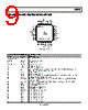


1. General Information:
️· Document: Partial excerpt from AD9626 datasheet.
️· Device: AD9626 (Analog-to-Digital Converter - ADC)
️· Operating Conditions: AVDD = 1.8V, DRVDD = 1.8V, Temperature range: -40°C to +85°C, fIN = -1.0 dBFS, Full Scale = 1.25V, DCS enabled.
️· Figures referenced: Figure 2 & 3 (likely related to switching characteristics).
2. Switching Specifications (Table 4):
This table defines various timing parameters. Here's a breakdown of the parameters and the ranges for the three AD9626 speeds (170, 210, and 250 MSPS - Mega Samples Per Second):
️· Maximum Conversion Rate: 170 / 210 / 250 MSPS
️· Minimum Conversion Rate: 170 / 210 / 250 MSPS
️· CLK+ Pulse Width High (tCH): 40 ns (constant across speeds)
️· CLK+ Pulse Width Low (tCL): 2.65 / 2.15 / 1.8 ns
️· Output, Single Data Port Mode: Data Propagation Delay (tPD): 2.65 / 2.15 / 1.8 ns
️· DCO Propagation Delay (tCPD): 2.9 ns (constant across speeds)
️· Data to DCO Skew (tSKEW): 2.9 ns (constant across speeds)
️· Latency: 3.7 cycles (constant)
️· Output, Interleaved Mode:
- Data Propagation Delay (tPDA, tPDB): 2.65 / 2.15 / 1.8 ns
- DCO Propagation Delay (tCPDA, tCPDB): 2.9 ns (constant)
- Data to DCO Skew (tSKEWA, tSKEWB): 2.9 ns (constant)
️· Standby Recovery: 3.4 µs (constant)
️· Power-Down Recovery: 6 cycles (constant)
️· Aperture Delay (tA): 0 ns
️· Aperture Uncertainty (Jitter, tJ): 0.3 / 0.55 / 1.1 ps rms (root mean square).
3. Logic Specifications (Table 1):
️· Maximum Conversion Rate: 170 / 210 / 250 MSPS
️· Minimum Conversion Rate: 170 / 210 / 250 MSPS
️· Maximum Conversion Rate: 170 / 210 / 250 MSPS
️· Logic Output High Level: DRVDD - 0.05V
️· Logic Output Low Level: GND + 0.05V
️· Input Logic High Level: 0.8 x AVDD
️· Input Logic Low Level: 0.2 x AVDD
️· Output Coding Options: Twos complement, Gray code, or offset binary (default).
Key Takeaways:
️· The AD9626 is a versatile ADC that can operate at different sampling rates (170, 210, and 250 MSPS).
️· The switching characteristics (timing parameters) change with the sampling rate.
️· The datasheet excerpt provides critical timing information needed for proper system design and interface control.
️· Output coding options are available.
1. General Information:
️· Document: Partial excerpt from AD9626 datasheet.
️· Device: AD9626 (Analog-to-Digital Converter - ADC)
️· Operating Conditions: AVDD = 1.8V, DRVDD = 1.8V, Temperature range: -40°C to +85°C, fIN = -1.0 dBFS, Full Scale = 1.25V, DCS enabled.
️· Figures referenced: Figure 2 & 3 (likely related to switching characteristics).
2. Switching Specifications (Table 4):
This table defines various timing parameters. Here's a breakdown of the parameters and the ranges for the three AD9626 speeds (170, 210, and 250 MSPS - Mega Samples Per Second):
️· Maximum Conversion Rate: 170 / 210 / 250 MSPS
️· Minimum Conversion Rate: 170 / 210 / 250 MSPS
️· CLK+ Pulse Width High (tCH): 40 ns (constant across speeds)
️· CLK+ Pulse Width Low (tCL): 2.65 / 2.15 / 1.8 ns
️· Output, Single Data Port Mode: Data Propagation Delay (tPD): 2.65 / 2.15 / 1.8 ns
️· DCO Propagation Delay (tCPD): 2.9 ns (constant across speeds)
️· Data to DCO Skew (tSKEW): 2.9 ns (constant across speeds)
️· Latency: 3.7 cycles (constant)
️· Output, Interleaved Mode:
- Data Propagation Delay (tPDA, tPDB): 2.65 / 2.15 / 1.8 ns
- DCO Propagation Delay (tCPDA, tCPDB): 2.9 ns (constant)
- Data to DCO Skew (tSKEWA, tSKEWB): 2.9 ns (constant)
️· Standby Recovery: 3.4 µs (constant)
️· Power-Down Recovery: 6 cycles (constant)
️· Aperture Delay (tA): 0 ns
️· Aperture Uncertainty (Jitter, tJ): 0.3 / 0.55 / 1.1 ps rms (root mean square).
3. Logic Specifications (Table 1):
️· Maximum Conversion Rate: 170 / 210 / 250 MSPS
️· Minimum Conversion Rate: 170 / 210 / 250 MSPS
️· Maximum Conversion Rate: 170 / 210 / 250 MSPS
️· Logic Output High Level: DRVDD - 0.05V
️· Logic Output Low Level: GND + 0.05V
️· Input Logic High Level: 0.8 x AVDD
️· Input Logic Low Level: 0.2 x AVDD
️· Output Coding Options: Twos complement, Gray code, or offset binary (default).
Key Takeaways:
️· The AD9626 is a versatile ADC that can operate at different sampling rates (170, 210, and 250 MSPS).
️· The switching characteristics (timing parameters) change with the sampling rate.
️· The datasheet excerpt provides critical timing information needed for proper system design and interface control.
️· Output coding options are available.
| Part No. | AD9626_15 |
| Manufacturer | AD |
| Size | 1Mb |
| Pages | 36 pages |
| Description | 12-Bit, 170 MSPS/210 MSPS/250 MSPS, 1.8 V Analog-to-Digital Converter |
| ALLDATASHEET é útil para você? [ DONATE ] |
Sobre Alldatasheet | Publicidade | Contato conosco | Privacy Policy | Link para a ficha técnica | roca de Link | Lista de Fabricantes All Rights Reserved©Alldatasheet.com |
| Russian : Alldatasheetru.com | Korean : Alldatasheet.co.kr | Spanish : Alldatasheet.es | French : Alldatasheet.fr | Italian : Alldatasheetit.com Portuguese : Alldatasheetpt.com | Polish : Alldatasheet.pl | Vietnamese : Alldatasheet.vn Indian : Alldatasheet.in | Mexican : Alldatasheet.com.mx | British : Alldatasheet.co.uk | New Zealand : Alldatasheet.co.nz |
|
Family Site : ic2ic.com |
icmetro.com |
 Portuguese ▼
  English
 Chinese
 German
 Japanese
 Russian
 Korean
 Spanish
 French
 Italian
 Polish
 Vietnamese
 Indian
 Mexican
 British
 New Zealand