 |
Os motores de busca de Datasheet de Componentes eletrônicos |
|
|
Os motores de busca de Datasheet de Componentes eletrônicos |
|
The question interval is too short.
Please try again in a few seconds.

Hello, Please ask a question about AD9012 Datasheet
# Example questions:
➢ What is the recommended bond wire material and bonding method for attaching the die to a substrate?
➢ What are the two options for the dynamic configuration of ad1 and ad2, and how do they differ from the static configuration?
➢ What is the metallization material used, and what is the substrate potential?
| Part No. | AD9012 |
| Manufacturer | AD |
| Size | 263 Kbytes |
| Pages | 8 pages |
| Description | High Speed 8-Bit TTL A/D Converter |




1. Product Overview & Functionality
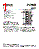
️· What it is: The AD9012 is an 8-bit Analog-to-Digital Converter (ADC). It's a key component for converting analog signals into digital representations.
️· Resolution: 8-bit resolution, meaning it can represent 256 discrete levels (0-255) of the input signal.
️· Applications: It's well-suited for applications like data acquisition systems, process control, and instrumentation.
2. Electrical Characteristics (Important Parameters)
️· Supply Voltages:
- Digital: -5.2V
- Analog: +5.0V
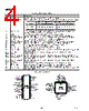
- Reference (AD1): -2.0V (Static Option) or dynamic (Waveforms provided in Figure 2 - Timing Diagram). The dynamic reference voltage is a key feature which allows for increased accuracy.
- AD2: +0.4V. The precise level depends on the chosen operation mode.
️· Accuracy: The datasheet specifies resistors and capacitors have tolerances of 5% and 20% respectively.
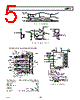
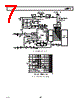
️· Input/Output Circuits: Figure 3 shows a schematic of the input and output circuits. It includes capacitors (0.1uF) and voltage levels.
3. Pin Configurations & Functions
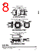
️· Key Pins (Refer to Figure 2: Pin Configurations):
- Digital Inputs & Outputs (D1-D8)
- Analog Input
- Analog Ground
- Encode
- Digital Supply (+VDS)
- Analog Supply (+VDS)
- Overflow Output
- Reference Inputs (AD1, AD2) – These are critical for accurate conversion.
- Digital Ground
4. Die Information (For Manufacturing/Integration)
️· Die Dimensions: 111 mils x 123 mils x 15 mils (±2 mils). This is crucial for packaging and board layout.
️· Metallization: Gold
️· Substrate Potential: -Vs (Important for grounding and noise considerations)
️· Bonding: Gold ball bonding
5. Key Features & Considerations
️· Dynamic Reference: The reference voltages (AD1, AD2) can be dynamic (changing over time). This is a key design characteristic that provides advantages in some applications. The dynamic reference is explained with waveforms in Figure 2.
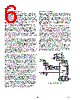
️· Burn-In Procedures: Figure 4 describes the burn-in procedures that are carried out on the parts to ensure quality.
️· Voltage Options:
- Option #1 (Static) uses fixed reference voltages: AD1 = -2.0V and AD2 = +0.4V
- Option #2 (Dynamic) allows for changes in these reference voltages over time, which provides higher performance.
️· Careful Design: The datasheet emphasizes the importance of careful design, including attention to grounding, noise reduction, and proper component selection.
6. Figures & Diagrams
️· Figure 4: Timing Diagram: Shows the timing relationship between the digital outputs and reference voltages.
️· Figure 4: Input/Output Circuits: Shows the overall input and output of the chip.
️· Figure 4: Pin Configurations: Depicts the physical arrangement of the pins on the chip.
️· Figure 4: Burn-In Diagram Shows burn-in procedures to ensure part reliability.
1. Product Overview & Functionality
️· What it is: The AD9012 is an 8-bit Analog-to-Digital Converter (ADC). It's a key component for converting analog signals into digital representations.
️· Resolution: 8-bit resolution, meaning it can represent 256 discrete levels (0-255) of the input signal.
️· Applications: It's well-suited for applications like data acquisition systems, process control, and instrumentation.
2. Electrical Characteristics (Important Parameters)
️· Supply Voltages:
- Digital: -5.2V
- Analog: +5.0V
- Reference (AD1): -2.0V (Static Option) or dynamic (Waveforms provided in Figure 2 - Timing Diagram). The dynamic reference voltage is a key feature which allows for increased accuracy.
- AD2: +0.4V. The precise level depends on the chosen operation mode.
️· Accuracy: The datasheet specifies resistors and capacitors have tolerances of 5% and 20% respectively.
️· Input/Output Circuits: Figure 3 shows a schematic of the input and output circuits. It includes capacitors (0.1uF) and voltage levels.
3. Pin Configurations & Functions
️· Key Pins (Refer to Figure 2: Pin Configurations):
- Digital Inputs & Outputs (D1-D8)
- Analog Input
- Analog Ground
- Encode
- Digital Supply (+VDS)
- Analog Supply (+VDS)
- Overflow Output
- Reference Inputs (AD1, AD2) – These are critical for accurate conversion.
- Digital Ground
4. Die Information (For Manufacturing/Integration)
️· Die Dimensions: 111 mils x 123 mils x 15 mils (±2 mils). This is crucial for packaging and board layout.
️· Metallization: Gold
️· Substrate Potential: -Vs (Important for grounding and noise considerations)
️· Bonding: Gold ball bonding
5. Key Features & Considerations
️· Dynamic Reference: The reference voltages (AD1, AD2) can be dynamic (changing over time). This is a key design characteristic that provides advantages in some applications. The dynamic reference is explained with waveforms in Figure 2.
️· Burn-In Procedures: Figure 4 describes the burn-in procedures that are carried out on the parts to ensure quality.
️· Voltage Options:
- Option #1 (Static) uses fixed reference voltages: AD1 = -2.0V and AD2 = +0.4V
- Option #2 (Dynamic) allows for changes in these reference voltages over time, which provides higher performance.
️· Careful Design: The datasheet emphasizes the importance of careful design, including attention to grounding, noise reduction, and proper component selection.
6. Figures & Diagrams
️· Figure 4: Timing Diagram: Shows the timing relationship between the digital outputs and reference voltages.
️· Figure 4: Input/Output Circuits: Shows the overall input and output of the chip.
️· Figure 4: Pin Configurations: Depicts the physical arrangement of the pins on the chip.
️· Figure 4: Burn-In Diagram Shows burn-in procedures to ensure part reliability.
| Part No. | AD9012 |
| Manufacturer | AD |
| Size | 263 Kbytes |
| Pages | 8 pages |
| Description | High Speed 8-Bit TTL A/D Converter |
| ALLDATASHEET é útil para você? [ DONATE ] |
Sobre Alldatasheet | Publicidade | Contato conosco | Privacy Policy | Link para a ficha técnica | roca de Link | Lista de Fabricantes All Rights Reserved©Alldatasheet.com |
| Russian : Alldatasheetru.com | Korean : Alldatasheet.co.kr | Spanish : Alldatasheet.es | French : Alldatasheet.fr | Italian : Alldatasheetit.com Portuguese : Alldatasheetpt.com | Polish : Alldatasheet.pl | Vietnamese : Alldatasheet.vn Indian : Alldatasheet.in | Mexican : Alldatasheet.com.mx | British : Alldatasheet.co.uk | New Zealand : Alldatasheet.co.nz |
|
Family Site : ic2ic.com |
icmetro.com |
 Portuguese ▼
  English
 Chinese
 German
 Japanese
 Russian
 Korean
 Spanish
 French
 Italian
 Polish
 Vietnamese
 Indian
 Mexican
 British
 New Zealand