Os motores de busca de Datasheet de Componentes eletrônicos
  Portuguese  ▼
ALLDATASHEETPT.COM

X  

AD8033AR Datasheet with Chat AI
  • AIauthorized

    Hello, Please ask a question about AD8033AR Datasheet

  • # Example questions: ➢ What is the maximum power dissipation for an ad8033/ad8034 in an 8-lead sot-23 package at an ambient temperature of 25°c? assume the thermal resistance (θja) for the sot-23 package is 160°c/w.
    ➢ What is the maximum junction temperature for the ad8033/ad8034, and why is exceeding it detrimental to the device's performance?
    ➢ The document warns against output short circuits. briefly explain why this is problematic and what the potential consequence is.

  • Part No.AD8033AR
    ManufacturerAD
    Size620 Kbytes
    Pages25 pages
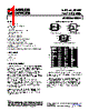
    DescriptionLow Cost, 80 MHz FastFET Op Amps
    Datasheet Summary with AI

    1. Device Identification:

    ️· Device Names: AD8033 / AD8034
    ️· Type: Op Amps (Operational Amplifiers)

    2. Absolute Maximum Ratings (Important - Don't Exceed These!)

    These are the *absolute* limits. Exceeding them can permanently damage the device.

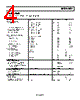
    Parameter Rating
    Supply Voltage (V<sub>S</sub>) 26.4 V
    Power Dissipation (P<sub>D</sub>) See Figure 5 (Dependent on package and ambient temperature)
    Common-Mode Input Voltage 26.4 V
    Differential Input Voltage 1.4 V
    Storage Temperature Range -65°C to +125°C
    Operating Temperature Range -40°C to +85°C
    | Lead Temperature (Soldering) | 300°C (for 10 seconds)

    3. Power Dissipation and Junction Temperature

    ️· Importance: The key is to keep the *junction temperature (T<sub>J</sub>)* within safe limits. Exceeding ~175°C can cause permanent damage.
    ️· Formula: _T<sub>J</sub>_ = _T<sub>A</sub>_ + (_P<sub>D</sub>_ × _θ<sub>JA</sub>_)
    - _T<sub>J</sub>_: Junction Temperature
    - _T<sub>A</sub>_: Ambient Temperature
    - _P<sub>D</sub>_: Power Dissipation (total power in the package)
    - _θ<sub>JA</sub>_: Thermal Resistance from Junction to Ambient (package-dependent)
    ️· Figure 5: This figure shows how much power the chip can dissipate based on the ambient temperature. This will vary with package type and PCB design.
    ️· Thermal Resistance: Better PCB design and heat sinks reduce _θ<sub>JA</sub>_.
    ️· Important Note: The text emphasizes minimizing parasitic capacitances at the input leads due to the high speed of the op amps.

    4. Output Short Circuit Considerations

    ️· Danger: Shorting the output or drawing excessive current can lead to catastrophic failure.
    ️· Recommendation: Avoid output short circuits.

    5. Packages and Thermal Resistance (θ<sub>JA</sub>) - Approximate Values

    Package θ<sub>JA</sub> (Thermal Resistance)
    SOIC-8 125°C/W
    SC70-5 210°C/W
    SOT-23-8 160°C/W

    6. Key Operating Conditions (Vary Depending on Which Table is Referenced)

    There are two different sets of operating conditions, which will vary depending on the supplies

    Parameter Table 1 Table 2
    Supply Voltage (V<sub>S</sub>) 26.4 V 26.4 V
    Common-Mode Input Voltage 26.4 V 26.4 V
    Differential Input Voltage 1.4 V 1.4 V
    Input Common-Mode Voltage Range ±5 V ±5 V
    Input Common-Mode Voltage Range −12.0 to +9.0 −12.0 to +9.0


    Summary of Important Considerations

    ️· Thermal Management: Critical for reliable operation. Monitor junction temperatures, consider PCB layout and heat sinking.
    ️· Output Short Circuits: Avoid them.
    ️· Input Capacitance: Minimize input lead capacitance due to the op amps high-speed operation.
    ️· Refer to Table 5: Use Table 5 for a better understanding of maximum power dissipation.
    ️· Reference Table 1 and 2: Review the operating conditions for both tables.

    1. Device Identification:

    ️· Device Names: AD8033 / AD8034
    ️· Type: Op Amps (Operational Amplifiers)

    2. Absolute Maximum Ratings (Important - Don't Exceed These!)

    These are the *absolute* limits. Exceeding them can permanently damage the device.

    Parameter Rating
    Supply Voltage (V<sub>S</sub>) 26.4 V
    Power Dissipation (P<sub>D</sub>) See Figure 5 (Dependent on package and ambient temperature)
    Common-Mode Input Voltage 26.4 V
    Differential Input Voltage 1.4 V
    Storage Temperature Range -65°C to +125°C
    Operating Temperature Range -40°C to +85°C
    | Lead Temperature (Soldering) | 300°C (for 10 seconds)

    3. Power Dissipation and Junction Temperature

    ️· Importance: The key is to keep the *junction temperature (T<sub>J</sub>)* within safe limits. Exceeding ~175°C can cause permanent damage.
    ️· Formula: _T<sub>J</sub>_ = _T<sub>A</sub>_ + (_P<sub>D</sub>_ × _θ<sub>JA</sub>_)
    - _T<sub>J</sub>_: Junction Temperature
    - _T<sub>A</sub>_: Ambient Temperature
    - _P<sub>D</sub>_: Power Dissipation (total power in the package)
    - _θ<sub>JA</sub>_: Thermal Resistance from Junction to Ambient (package-dependent)
    ️· Figure 5: This figure shows how much power the chip can dissipate based on the ambient temperature. This will vary with package type and PCB design.
    ️· Thermal Resistance: Better PCB design and heat sinks reduce _θ<sub>JA</sub>_.
    ️· Important Note: The text emphasizes minimizing parasitic capacitances at the input leads due to the high speed of the op amps.

    4. Output Short Circuit Considerations

    ️· Danger: Shorting the output or drawing excessive current can lead to catastrophic failure.
    ️· Recommendation: Avoid output short circuits.

    5. Packages and Thermal Resistance (θ<sub>JA</sub>) - Approximate Values

    Package θ<sub>JA</sub> (Thermal Resistance)
    SOIC-8 125°C/W
    SC70-5 210°C/W
    SOT-23-8 160°C/W

    6. Key Operating Conditions (Vary Depending on Which Table is Referenced)

    There are two different sets of operating conditions, which will vary depending on the supplies

    Parameter Table 1 Table 2
    Supply Voltage (V<sub>S</sub>) 26.4 V 26.4 V
    Common-Mode Input Voltage 26.4 V 26.4 V
    Differential Input Voltage 1.4 V 1.4 V
    Input Common-Mode Voltage Range ±5 V ±5 V
    Input Common-Mode Voltage Range −12.0 to +9.0 −12.0 to +9.0


    Summary of Important Considerations

    ️· Thermal Management: Critical for reliable operation. Monitor junction temperatures, consider PCB layout and heat sinking.
    ️· Output Short Circuits: Avoid them.
    ️· Input Capacitance: Minimize input lead capacitance due to the op amps high-speed operation.
    ️· Refer to Table 5: Use Table 5 for a better understanding of maximum power dissipation.
    ️· Reference Table 1 and 2: Review the operating conditions for both tables.

    Part No.AD8033AR
    ManufacturerAD
    Size620 Kbytes
    Pages25 pages
    DescriptionLow Cost, 80 MHz FastFET Op Amps
    ALLDATASHEET é útil para você?  [ DONATE ] 

    Sobre Alldatasheet   |   Publicidade   |   Contato conosco   |   Privacy Policy   |   Link para a ficha técnica    |   roca de Link   |   Lista de Fabricantes
    All Rights Reserved©Alldatasheet.com


    Mirror Sites
    English : Alldatasheet.com  |   English : Alldatasheet.net  |   Chinese : Alldatasheetcn.com  |   German : Alldatasheetde.com  |   Japanese : Alldatasheet.jp
    Russian : Alldatasheetru.com  |   Korean : Alldatasheet.co.kr  |   Spanish : Alldatasheet.es  |   French : Alldatasheet.fr  |   Italian : Alldatasheetit.com
    Portuguese : Alldatasheetpt.com  |   Polish : Alldatasheet.pl  |   Vietnamese : Alldatasheet.vn
    Indian : Alldatasheet.in  |   Mexican : Alldatasheet.com.mx  |   British : Alldatasheet.co.uk  |   New Zealand : Alldatasheet.co.nz
    Family Site : ic2ic.com  |   icmetro.com