 |
Os motores de busca de Datasheet de Componentes eletrônicos |
|
|
Os motores de busca de Datasheet de Componentes eletrônicos |
|
The question interval is too short.
Please try again in a few seconds.

Hello, Please ask a question about AD9764-EB Datasheet
# Example questions:
➢ What does the specification 'glitch impulse' measure, and in what units is it typically expressed?
➢ What is the purpose of connecting a 0.1µf capacitor between comp1 and avdd?
➢ What is the acceptable range for the analog supply voltage (avdd)?
| Part No. | AD9764-EB |
| Manufacturer | AD |
| Size | 314 Kbytes |
| Pages | 22 pages |
| Description | 14-Bit, 125 MSPS TxDAC D/A Converter |




1. Overview
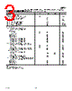
️· Device: AD9764 is a DAC (Digital-to-Analog Converter). It's likely part of a larger system, given the numerous connections and references.
️· Type: It appears to be a current-output DAC (I OUTA and I OUTB, providing complementary output currents).
️· Function: Converts digital signals into analog current signals.
2. Pin Configuration and Functionality (Very Detailed)
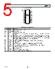
️· Data Inputs (DB13 - DB0): These are the digital input bits that define the analog output value. MSB (Most Significant Bit) is DB13, LSB (Least Significant Bit) is DB0.
️· Clock (CLOCK): The data is latched (captured) on the positive edge of this clock signal.
️· Sleep (SLEEP): Power-down control. Active high (when the voltage is high). It includes a pull-down circuit.
️· Reference Voltages & Ground (REFLO, REFIO, ACOM, AVDD, DCOM, DVDD): These are crucial for setting the operating voltage levels and reference for the DAC. REFIO can be used as an input reference or an output (1.2V).
️· Full Scale Adjustment (FS ADJ): Allows fine-tuning of the output range.
️· Analog Outputs (I OUTA, I OUTB): The complementary current outputs representing the analog value.
️· COMP1 & COMP2: Likely related to internal comparators or buffering circuitry.
️· NC (No Connection): Indicates a pin that is not connected internally and can be left floating.
3. Specifications & Performance Characteristics
️· Linearity Error: How closely the actual output follows a straight-line relationship to the digital input.
️· Differential Nonlinearity (DNL): Variation in analog value for a single-bit change in the digital input.
️· Offset Error: Deviation of the output from zero when all inputs are zero.
️· Gain Error: Difference between the actual output range and the ideal output range.
️· Output Compliance Range: The allowable voltage range for the output currents, to prevent saturation or breakdown.
️· Temperature Drift: How the specifications change with temperature.
️· Power Supply Rejection: How the DAC's performance is affected by variations in the supply voltages.
️· Settling Time: Time required for the output to reach a stable value.
️· Glitch Impulse: Undesired transient spikes in the output.
️· Spurious-Free Dynamic Range (SFDR): Measures how much noise and unwanted signals are present in the output.
️· Total Harmonic Distortion (THD): Quantifies the amount of harmonic distortion in the output signal.
️· Multitone Power Ratio: measures the SFDR for an output containing multiple carrier tones.
4. Important Terminology & Concepts
️· DAC: Digital-to-Analog Converter
️· MSB/LSB: Most Significant Bit / Least Significant Bit
️· SFDR: Spurious Free Dynamic Range
️· THD: Total Harmonic Distortion
️· Complementary Outputs: Output signals that are opposite to each other (I OUTA & I OUTB).
️· Compliance Voltage: The maximum voltage the output can handle.
5. Test Setup (Figure 7):
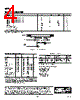
️· The figure depicts a typical AC characterization test setup. It includes components like spectrum/network analyzers, input sources, and reference points. It suggests how the DAC is tested for its performance.
Key Takeaways for Practical Use:
️· Power Supply Importance: The AD9764 requires careful attention to the power supply voltages (DVDD, DCOM, AVDD) and reference voltages (REFLO, REFIO).
️· Compliance: Ensure the output compliance voltage is within the specified limits to avoid distortions.
️· Noise and Distortion: Pay attention to the SFDR and THD specifications to minimize noise and distortion in the analog output.
1. Overview
️· Device: AD9764 is a DAC (Digital-to-Analog Converter). It's likely part of a larger system, given the numerous connections and references.
️· Type: It appears to be a current-output DAC (I OUTA and I OUTB, providing complementary output currents).
️· Function: Converts digital signals into analog current signals.
2. Pin Configuration and Functionality (Very Detailed)
️· Data Inputs (DB13 - DB0): These are the digital input bits that define the analog output value. MSB (Most Significant Bit) is DB13, LSB (Least Significant Bit) is DB0.
️· Clock (CLOCK): The data is latched (captured) on the positive edge of this clock signal.
️· Sleep (SLEEP): Power-down control. Active high (when the voltage is high). It includes a pull-down circuit.
️· Reference Voltages & Ground (REFLO, REFIO, ACOM, AVDD, DCOM, DVDD): These are crucial for setting the operating voltage levels and reference for the DAC. REFIO can be used as an input reference or an output (1.2V).
️· Full Scale Adjustment (FS ADJ): Allows fine-tuning of the output range.
️· Analog Outputs (I OUTA, I OUTB): The complementary current outputs representing the analog value.
️· COMP1 & COMP2: Likely related to internal comparators or buffering circuitry.
️· NC (No Connection): Indicates a pin that is not connected internally and can be left floating.
3. Specifications & Performance Characteristics
️· Linearity Error: How closely the actual output follows a straight-line relationship to the digital input.
️· Differential Nonlinearity (DNL): Variation in analog value for a single-bit change in the digital input.
️· Offset Error: Deviation of the output from zero when all inputs are zero.
️· Gain Error: Difference between the actual output range and the ideal output range.
️· Output Compliance Range: The allowable voltage range for the output currents, to prevent saturation or breakdown.
️· Temperature Drift: How the specifications change with temperature.
️· Power Supply Rejection: How the DAC's performance is affected by variations in the supply voltages.
️· Settling Time: Time required for the output to reach a stable value.
️· Glitch Impulse: Undesired transient spikes in the output.
️· Spurious-Free Dynamic Range (SFDR): Measures how much noise and unwanted signals are present in the output.
️· Total Harmonic Distortion (THD): Quantifies the amount of harmonic distortion in the output signal.
️· Multitone Power Ratio: measures the SFDR for an output containing multiple carrier tones.
4. Important Terminology & Concepts
️· DAC: Digital-to-Analog Converter
️· MSB/LSB: Most Significant Bit / Least Significant Bit
️· SFDR: Spurious Free Dynamic Range
️· THD: Total Harmonic Distortion
️· Complementary Outputs: Output signals that are opposite to each other (I OUTA & I OUTB).
️· Compliance Voltage: The maximum voltage the output can handle.
5. Test Setup (Figure 7):
️· The figure depicts a typical AC characterization test setup. It includes components like spectrum/network analyzers, input sources, and reference points. It suggests how the DAC is tested for its performance.
Key Takeaways for Practical Use:
️· Power Supply Importance: The AD9764 requires careful attention to the power supply voltages (DVDD, DCOM, AVDD) and reference voltages (REFLO, REFIO).
️· Compliance: Ensure the output compliance voltage is within the specified limits to avoid distortions.
️· Noise and Distortion: Pay attention to the SFDR and THD specifications to minimize noise and distortion in the analog output.
| Part No. | AD9764-EB |
| Manufacturer | AD |
| Size | 314 Kbytes |
| Pages | 22 pages |
| Description | 14-Bit, 125 MSPS TxDAC D/A Converter |
| ALLDATASHEET é útil para você? [ DONATE ] |
Sobre Alldatasheet | Publicidade | Contato conosco | Privacy Policy | Link para a ficha técnica | roca de Link | Lista de Fabricantes All Rights Reserved©Alldatasheet.com |
| Russian : Alldatasheetru.com | Korean : Alldatasheet.co.kr | Spanish : Alldatasheet.es | French : Alldatasheet.fr | Italian : Alldatasheetit.com Portuguese : Alldatasheetpt.com | Polish : Alldatasheet.pl | Vietnamese : Alldatasheet.vn Indian : Alldatasheet.in | Mexican : Alldatasheet.com.mx | British : Alldatasheet.co.uk | New Zealand : Alldatasheet.co.nz |
|
Family Site : ic2ic.com |
icmetro.com |
 Portuguese ▼
  English
 Chinese
 German
 Japanese
 Russian
 Korean
 Spanish
 French
 Italian
 Polish
 Vietnamese
 Indian
 Mexican
 British
 New Zealand