 |
Os motores de busca de Datasheet de Componentes eletrônicos |
|
|
Os motores de busca de Datasheet de Componentes eletrônicos |
|
The question interval is too short.
Please try again in a few seconds.

Hello, Please ask a question about TSX561AILT Datasheet
# Example questions:
➢ What is the guaranteed maximum supply current (icc) per channel at 25°c with a vcc+ of 5v, and what is the equivalent value for vcc+ of 5v?
➢ What is the typical input offset voltage (vio) for the tsx56xa at 25°c with a vcc+ of 5v?
➢ How does the slew rate (sr) change when vcc+ is increased from 5v to 5v, comparing the values provided in table 5 and table 4?
| Part No. | TSX561AILT |
| Manufacturer | STMICROELECTRONICS |
| Size | 1Mb |
| Pages | 27 pages |
| Description | Micropower, wide bandwidth (900 kHz), 16 V CMOS operational amplifiers |




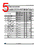
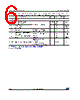
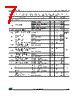


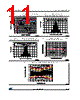
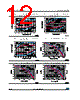
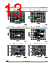
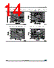

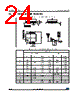
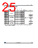
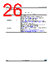

1. General Information
️· Two Voltage Supply Options: The datasheet provides specifications for operation at both +5V and +3.3V (inferred from the two tables).
️· Test Conditions: Most specifications are given with `VCC- = 0V`, `VCC+` at either 3.3V or 5V, `VCM = VCC+/2`, `RL = 10kΩ`, and `T` at 25°C unless otherwise noted.
️· Guaranteed by Design/Typical Values: Some values are "Guaranteed by Design" and others are stated as "Typical".
2. Key DC Performance Parameters (Summarized for both 3.3V & 5V)
️· Input Offset Voltage (Vio):
- 3.3V: Typically 600µV (TSX56xA), 1mV (TSX56x) at 25°C, up to 1800µV at -40°C to +125°C
- 5V: Typically 600µV (TSX56xA), 1mV (TSX56x) at 25°C, up to 1800µV at -40°C to +125°C
️· Input Offset Voltage Drift (ΔVio/ΔT): 2-12 µV/°C (over -40°C to +125°C).
️· Long-term Input Offset Voltage Drift (ΔVio): For 5V supply, 5 nV/month.
️· Input Bias Current (Iib): 1-100 pA typical.
️· Input Offset Current (Iio): 1-100 pA typical.
️· Common Mode Rejection Ratio (CMRR):
- 3.3V: 66-84 dB (TSX56xA), 50-69 dB (TSX56x)
- 5V: 66-84 dB (TSX56xA), 50-69 dB (TSX56x)
️· Large Signal Voltage Gain (Avd): 85 dB (typical)
️· Output Voltage Swing (VOH/VOL): (with 10kΩ load) approximately 70mV and 100mV
️· Supply Current (ICC): 235-350µA (3.3V), 235-400µA (5V)
3. AC Performance Parameters
️· Gain Bandwidth Product (GBP): 700-850 kHz (3.3V), 700-850 kHz (5V).
️· Unity Gain Frequency (Fu): 730 kHz (3.3V), 730 kHz (5V)
️· Phase Margin (Φm): 55°
️· Gain Margin (Gm): 9°
️· Slew Rate (SR): 1.1 V/µs (5V supply)
️· Low Frequency Peak-to-Peak Input Noise (∫en): 15-15 µVpp
️· Equivalent Input Noise Voltage Density (en): 55 nV/√Hz @ 1kHz, 29 nV/√Hz @ 10kHz
️· Total Harmonic Distortion + Noise (THD+N): 0.002% - 0.003%
4. Important Notes/Caveats
️· TSX56xA vs. TSX56x: There's a distinction between these two variants. The TSX56xA generally has better specs (lower offset voltages, better CMRR).
️· Temperature Effects: Performance parameters are significantly impacted by temperature.
️· Long-Term Drift: The datasheet notes a long-term offset voltage drift, particularly for the 5V supply.
1. General Information
️· Two Voltage Supply Options: The datasheet provides specifications for operation at both +5V and +3.3V (inferred from the two tables).
️· Test Conditions: Most specifications are given with `VCC- = 0V`, `VCC+` at either 3.3V or 5V, `VCM = VCC+/2`, `RL = 10kΩ`, and `T` at 25°C unless otherwise noted.
️· Guaranteed by Design/Typical Values: Some values are "Guaranteed by Design" and others are stated as "Typical".
2. Key DC Performance Parameters (Summarized for both 3.3V & 5V)
️· Input Offset Voltage (Vio):
- 3.3V: Typically 600µV (TSX56xA), 1mV (TSX56x) at 25°C, up to 1800µV at -40°C to +125°C
- 5V: Typically 600µV (TSX56xA), 1mV (TSX56x) at 25°C, up to 1800µV at -40°C to +125°C
️· Input Offset Voltage Drift (ΔVio/ΔT): 2-12 µV/°C (over -40°C to +125°C).
️· Long-term Input Offset Voltage Drift (ΔVio): For 5V supply, 5 nV/month.
️· Input Bias Current (Iib): 1-100 pA typical.
️· Input Offset Current (Iio): 1-100 pA typical.
️· Common Mode Rejection Ratio (CMRR):
- 3.3V: 66-84 dB (TSX56xA), 50-69 dB (TSX56x)
- 5V: 66-84 dB (TSX56xA), 50-69 dB (TSX56x)
️· Large Signal Voltage Gain (Avd): 85 dB (typical)
️· Output Voltage Swing (VOH/VOL): (with 10kΩ load) approximately 70mV and 100mV
️· Supply Current (ICC): 235-350µA (3.3V), 235-400µA (5V)
3. AC Performance Parameters
️· Gain Bandwidth Product (GBP): 700-850 kHz (3.3V), 700-850 kHz (5V).
️· Unity Gain Frequency (Fu): 730 kHz (3.3V), 730 kHz (5V)
️· Phase Margin (Φm): 55°
️· Gain Margin (Gm): 9°
️· Slew Rate (SR): 1.1 V/µs (5V supply)
️· Low Frequency Peak-to-Peak Input Noise (∫en): 15-15 µVpp
️· Equivalent Input Noise Voltage Density (en): 55 nV/√Hz @ 1kHz, 29 nV/√Hz @ 10kHz
️· Total Harmonic Distortion + Noise (THD+N): 0.002% - 0.003%
4. Important Notes/Caveats
️· TSX56xA vs. TSX56x: There's a distinction between these two variants. The TSX56xA generally has better specs (lower offset voltages, better CMRR).
️· Temperature Effects: Performance parameters are significantly impacted by temperature.
️· Long-Term Drift: The datasheet notes a long-term offset voltage drift, particularly for the 5V supply.
| Part No. | TSX561AILT |
| Manufacturer | STMICROELECTRONICS |
| Size | 1Mb |
| Pages | 27 pages |
| Description | Micropower, wide bandwidth (900 kHz), 16 V CMOS operational amplifiers |
| ALLDATASHEET é útil para você? [ DONATE ] |
Sobre Alldatasheet | Publicidade | Contato conosco | Privacy Policy | Link para a ficha técnica | roca de Link | Lista de Fabricantes All Rights Reserved©Alldatasheet.com |
| Russian : Alldatasheetru.com | Korean : Alldatasheet.co.kr | Spanish : Alldatasheet.es | French : Alldatasheet.fr | Italian : Alldatasheetit.com Portuguese : Alldatasheetpt.com | Polish : Alldatasheet.pl | Vietnamese : Alldatasheet.vn Indian : Alldatasheet.in | Mexican : Alldatasheet.com.mx | British : Alldatasheet.co.uk | New Zealand : Alldatasheet.co.nz |
|
Family Site : ic2ic.com |
icmetro.com |
 Portuguese ▼
  English
 Chinese
 German
 Japanese
 Russian
 Korean
 Spanish
 French
 Italian
 Polish
 Vietnamese
 Indian
 Mexican
 British
 New Zealand