 |
Os motores de busca de Datasheet de Componentes eletrônicos |
|
|
Os motores de busca de Datasheet de Componentes eletrônicos |
|
The question interval is too short.
Please try again in a few seconds.

Hello, Please ask a question about AOW10N65 Datasheet
# Example questions:
➢ What do the curves represent and how are they useful for thermal design?
➢ The document states a limitation regarding the use of these devices in life support systems. explain this disclaimer.
➢ What is the maximum junction temperature (tj(max)) specified for the aow10n65/aowf10n65 mosfets?
| Part No. | AOW10N65 |
| Manufacturer | AOSMD |
| Size | 347 Kbytes |
| Pages | 6 pages |
| Description | 650V,10A N-Channel MOSFET |

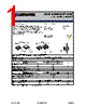
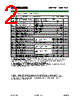

1. General Information
️· Device Type: N-Channel MOSFET
️· Target Market: Consumer market (not for life-support devices)
️· Important Disclaimer: AOS (the manufacturer) doesn't assume liability for use in critical applications (like life support).
️· Design Changes: AOS reserves the right to change the design without notice.
️· Variants: AOW10N65 and AOWF10N65 are two variants; the datasheet provides some shared and distinct characteristics for each. The "F" variant likely represents a different manufacturing process or slight design variation.
2. Electrical Characteristics (Typical Values @ 25°C unless noted)
️· Vds (Drain-Source Voltage): Can handle a significant voltage (check the datasheet for the maximum voltage rating, it varies slightly depending on the variant)
️· Vgs (Gate-Source Voltage): Voltage applied to the gate.
️· Id (Drain Current): The current flowing through the device. Limited by power dissipation and junction temperature.
️· Rds(on) (Drain-Source On-Resistance): A critical parameter. Lower Rds(on) means less power dissipation and higher efficiency.
️· Vgs(th) (Gate-Source Threshold Voltage): The voltage needed to start conducting.
️· Input Capacitance (Ciss, Cgs, Cgd): Capacitance values affect switching speed. Lower is generally better for high-frequency applications.
️· Output Capacitance (Coss): Impacts switching losses.
️· Gate Charge (Qg): Represents total gate charge. Impacts driving requirements.
3. Thermal Characteristics
️· Junction-to-Case Thermal Resistance (RθJC): Measures the device's ability to dissipate heat from the junction to the case.
️· Case-to-Ambient Thermal Resistance (RθJA): Measures the device's ability to dissipate heat from the case to the surrounding environment. Lower RθJA is better for heat dissipation.
️· Maximum Junction Temperature (Tj(max)): The maximum safe operating temperature of the junction. Exceeding this temperature can damage the device.
️· Power Dissipation (Pd): Maximum power the device can dissipate safely. Dependent on junction temperature and thermal resistances.
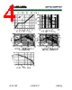
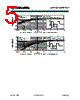
️· Transient Thermal Impedance (Normalized): A graph (Figures 12 & 9) showing how the junction temperature responds to pulsed power dissipation. Used for determining safe pulse widths and duty cycles.
4. Safe Operating Area (SOA)
️· SOA Graph (Figure 10): A key graph that defines the maximum drain voltage (Vds) that the device can handle for a given drain current (Id) while keeping the junction temperature below the maximum. This helps determine safe operating conditions.
️· Current De-rating (Figure 11): Shows how the maximum drain current decreases as the case temperature increases. This provides guidelines for thermal management.
5. Test Conditions & Notes
️· Repetitive Ratings: Ratings are based on low frequency and duty cycles to keep initial junction temperature below maximum.
️· Pulse Width: Values based on a given pulse width.
️· SOA Conditions: SOAs are based on junction temperature limits.
️· Thermal Resistance Measurements: RθJA is measured in a still air environment at 25°C.
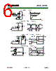
️· Test Circuits: The datasheet includes diagrams of test circuits used to measure various parameters (gate charge, diode recovery, UIS).
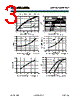
️· Fig. 1 - On-Region Characteristics: Provides a visualization of the on-resistance behavior across the drain current.
️· Figure 6 - Body-Diode Characteristics: Illustrates the forward voltage characteristics of the parasitic diode.
Key Differences between AOW10N65 and AOWF10N65
The primary differences aren't explicitly stated in the datasheet, suggesting they share most electrical characteristics. However, the subtle designation of "F" often indicates a different manufacturing process that might lead to minor variations in parameters or improved reliability.
1. General Information
️· Device Type: N-Channel MOSFET
️· Target Market: Consumer market (not for life-support devices)
️· Important Disclaimer: AOS (the manufacturer) doesn't assume liability for use in critical applications (like life support).
️· Design Changes: AOS reserves the right to change the design without notice.
️· Variants: AOW10N65 and AOWF10N65 are two variants; the datasheet provides some shared and distinct characteristics for each. The "F" variant likely represents a different manufacturing process or slight design variation.
2. Electrical Characteristics (Typical Values @ 25°C unless noted)
️· Vds (Drain-Source Voltage): Can handle a significant voltage (check the datasheet for the maximum voltage rating, it varies slightly depending on the variant)
️· Vgs (Gate-Source Voltage): Voltage applied to the gate.
️· Id (Drain Current): The current flowing through the device. Limited by power dissipation and junction temperature.
️· Rds(on) (Drain-Source On-Resistance): A critical parameter. Lower Rds(on) means less power dissipation and higher efficiency.
️· Vgs(th) (Gate-Source Threshold Voltage): The voltage needed to start conducting.
️· Input Capacitance (Ciss, Cgs, Cgd): Capacitance values affect switching speed. Lower is generally better for high-frequency applications.
️· Output Capacitance (Coss): Impacts switching losses.
️· Gate Charge (Qg): Represents total gate charge. Impacts driving requirements.
3. Thermal Characteristics
️· Junction-to-Case Thermal Resistance (RθJC): Measures the device's ability to dissipate heat from the junction to the case.
️· Case-to-Ambient Thermal Resistance (RθJA): Measures the device's ability to dissipate heat from the case to the surrounding environment. Lower RθJA is better for heat dissipation.
️· Maximum Junction Temperature (Tj(max)): The maximum safe operating temperature of the junction. Exceeding this temperature can damage the device.
️· Power Dissipation (Pd): Maximum power the device can dissipate safely. Dependent on junction temperature and thermal resistances.
️· Transient Thermal Impedance (Normalized): A graph (Figures 12 & 9) showing how the junction temperature responds to pulsed power dissipation. Used for determining safe pulse widths and duty cycles.
4. Safe Operating Area (SOA)
️· SOA Graph (Figure 10): A key graph that defines the maximum drain voltage (Vds) that the device can handle for a given drain current (Id) while keeping the junction temperature below the maximum. This helps determine safe operating conditions.
️· Current De-rating (Figure 11): Shows how the maximum drain current decreases as the case temperature increases. This provides guidelines for thermal management.
5. Test Conditions & Notes
️· Repetitive Ratings: Ratings are based on low frequency and duty cycles to keep initial junction temperature below maximum.
️· Pulse Width: Values based on a given pulse width.
️· SOA Conditions: SOAs are based on junction temperature limits.
️· Thermal Resistance Measurements: RθJA is measured in a still air environment at 25°C.
️· Test Circuits: The datasheet includes diagrams of test circuits used to measure various parameters (gate charge, diode recovery, UIS).
️· Fig. 1 - On-Region Characteristics: Provides a visualization of the on-resistance behavior across the drain current.
️· Figure 6 - Body-Diode Characteristics: Illustrates the forward voltage characteristics of the parasitic diode.
Key Differences between AOW10N65 and AOWF10N65
The primary differences aren't explicitly stated in the datasheet, suggesting they share most electrical characteristics. However, the subtle designation of "F" often indicates a different manufacturing process that might lead to minor variations in parameters or improved reliability.
| Part No. | AOW10N65 |
| Manufacturer | AOSMD |
| Size | 347 Kbytes |
| Pages | 6 pages |
| Description | 650V,10A N-Channel MOSFET |
| ALLDATASHEET é útil para você? [ DONATE ] |
Sobre Alldatasheet | Publicidade | Contato conosco | Privacy Policy | Link para a ficha técnica | roca de Link | Lista de Fabricantes All Rights Reserved©Alldatasheet.com |
| Russian : Alldatasheetru.com | Korean : Alldatasheet.co.kr | Spanish : Alldatasheet.es | French : Alldatasheet.fr | Italian : Alldatasheetit.com Portuguese : Alldatasheetpt.com | Polish : Alldatasheet.pl | Vietnamese : Alldatasheet.vn Indian : Alldatasheet.in | Mexican : Alldatasheet.com.mx | British : Alldatasheet.co.uk | New Zealand : Alldatasheet.co.nz |
|
Family Site : ic2ic.com |
icmetro.com |
 Portuguese ▼
  English
 Chinese
 German
 Japanese
 Russian
 Korean
 Spanish
 French
 Italian
 Polish
 Vietnamese
 Indian
 Mexican
 British
 New Zealand