 |
Os motores de busca de Datasheet de Componentes eletrônicos |
|
|
Os motores de busca de Datasheet de Componentes eletrônicos |
|
The question interval is too short.
Please try again in a few seconds.

Hello, Please ask a question about AD9754 Datasheet
# Example questions:
➢ What is the purpose of the fs adj pin, and what does it adjust?
➢ What is the acceptable range for the analog supply voltage (avdd)?
➢ How is total harmonic distortion (thd) expressed?
| Part No. | AD9754 |
| Manufacturer | AD |
| Size | 327 Kbytes |
| Pages | 24 pages |
| Description | 14-Bit, 125 MSPS High Performance TxDAC D/A Converter |








1. Overview & Product:
️· Product: AD9754 - This is a high-resolution DAC (Digital-to-Analog Converter).
️· Core Function: Converts digital data into an analog current output.
️· Key Features (Implied):
- High resolution (implied by detailed linearity specs)
- Current output (IOUTA and IOUTB)
- Flexible reference options (internal and external)
- Designed for precision applications (evident from stringent specifications)
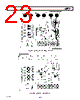
2. Pin Configuration and Functions (Important for Interfacing):
️· DB13-DB0: Data input bits (MSB to LSB).
️· CLOCK: Clock input. Data is latched on the positive edge.
️· DVDD: Digital supply voltage (2.7V to 5.5V).
️· DCOM: Digital common.
️· AVDD: Analog supply voltage (4.5V to 5.5V).
️· ACOM: Analog common.
️· IOUTA: Positive DAC current output.
️· IOUTB: Complementary DAC current output.
️· ICOMP: Internal bias node; decouple to ACOM with a 0.1µF capacitor.
️· REFLO: Reference ground (or used to disable internal reference).
️· REFIO: Reference input/output, configurable.
️· FS ADJ: Full-Scale Current Output Adjust.
️· SLEEP: Power-down control input.
️· NC: No connect (leave unconnected).
3. Specifications (Key Performance Metrics):
This section is extensive. Here's a summarized view of critical parameters. *Note: specific numerical values are not provided, only descriptions of the spec.*
️· Linearity Error: Maximum deviation from an ideal straight-line output.
️· Differential Nonlinearity (DNL): Variation in analog value per LSB change.
️· Offset Error: Deviation of output from zero current.
️· Gain Error: Difference between actual and ideal output span.
️· Temperature Drift: Change in parameters with temperature (expressed in ppm/°C).
️· Power Supply Rejection: How well the DAC's output is immune to changes in supply voltages.
️· Settling Time: Time to reach a stable output.
️· Glitch Impulse: Transients in the output caused by switching.
️· Spurious-Free Dynamic Range (SFDR): Difference between signal strength and spurious signals.
️· Total Harmonic Distortion (THD): Measure of harmonic distortion.
️· Multitone Power Ratio: SFDR for multiple carrier tones.
4. Definitions & Test Setup:
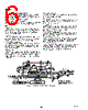
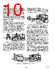
️· Basic AC Characterization Test Setup: A diagram showing how to connect the AD9754 to a spectrum analyzer for testing. (Important for validation and troubleshooting)
️· Segmented Switches: Indicates a design where different sections of the DAC's circuitry use separate switches for data inputs.
Key Takeaways for Practical Use:
️· Careful Power Supply Decoupling: Crucial for stable operation (mention of 0.1µF capacitors).
️· Reference Configuration: Flexible reference options require attention to connection (tie REFLO to AVDD or connect to ACOM).
️· Compliance Range: Ensure the output voltage (compliance) remains within the acceptable range to prevent saturation or breakdown.
️· ESD Sensitivity: Handle the device with caution to avoid electrostatic discharge damage.
To fully utilize this information, you would need to:
️· Consult the full datasheet: This excerpt is just a small part of the complete document.
️· Understand the specific application: The relevant specifications and design considerations will depend on the intended use of the AD9754.
️· Use the test setup diagram: To properly characterize the device's performance.
1. Overview & Product:
️· Product: AD9754 - This is a high-resolution DAC (Digital-to-Analog Converter).
️· Core Function: Converts digital data into an analog current output.
️· Key Features (Implied):
- High resolution (implied by detailed linearity specs)
- Current output (IOUTA and IOUTB)
- Flexible reference options (internal and external)
- Designed for precision applications (evident from stringent specifications)
2. Pin Configuration and Functions (Important for Interfacing):
️· DB13-DB0: Data input bits (MSB to LSB).
️· CLOCK: Clock input. Data is latched on the positive edge.
️· DVDD: Digital supply voltage (2.7V to 5.5V).
️· DCOM: Digital common.
️· AVDD: Analog supply voltage (4.5V to 5.5V).
️· ACOM: Analog common.
️· IOUTA: Positive DAC current output.
️· IOUTB: Complementary DAC current output.
️· ICOMP: Internal bias node; decouple to ACOM with a 0.1µF capacitor.
️· REFLO: Reference ground (or used to disable internal reference).
️· REFIO: Reference input/output, configurable.
️· FS ADJ: Full-Scale Current Output Adjust.
️· SLEEP: Power-down control input.
️· NC: No connect (leave unconnected).
3. Specifications (Key Performance Metrics):
This section is extensive. Here's a summarized view of critical parameters. *Note: specific numerical values are not provided, only descriptions of the spec.*
️· Linearity Error: Maximum deviation from an ideal straight-line output.
️· Differential Nonlinearity (DNL): Variation in analog value per LSB change.
️· Offset Error: Deviation of output from zero current.
️· Gain Error: Difference between actual and ideal output span.
️· Temperature Drift: Change in parameters with temperature (expressed in ppm/°C).
️· Power Supply Rejection: How well the DAC's output is immune to changes in supply voltages.
️· Settling Time: Time to reach a stable output.
️· Glitch Impulse: Transients in the output caused by switching.
️· Spurious-Free Dynamic Range (SFDR): Difference between signal strength and spurious signals.
️· Total Harmonic Distortion (THD): Measure of harmonic distortion.
️· Multitone Power Ratio: SFDR for multiple carrier tones.
4. Definitions & Test Setup:
️· Basic AC Characterization Test Setup: A diagram showing how to connect the AD9754 to a spectrum analyzer for testing. (Important for validation and troubleshooting)
️· Segmented Switches: Indicates a design where different sections of the DAC's circuitry use separate switches for data inputs.
Key Takeaways for Practical Use:
️· Careful Power Supply Decoupling: Crucial for stable operation (mention of 0.1µF capacitors).
️· Reference Configuration: Flexible reference options require attention to connection (tie REFLO to AVDD or connect to ACOM).
️· Compliance Range: Ensure the output voltage (compliance) remains within the acceptable range to prevent saturation or breakdown.
️· ESD Sensitivity: Handle the device with caution to avoid electrostatic discharge damage.
To fully utilize this information, you would need to:
️· Consult the full datasheet: This excerpt is just a small part of the complete document.
️· Understand the specific application: The relevant specifications and design considerations will depend on the intended use of the AD9754.
️· Use the test setup diagram: To properly characterize the device's performance.
| Part No. | AD9754 |
| Manufacturer | AD |
| Size | 327 Kbytes |
| Pages | 24 pages |
| Description | 14-Bit, 125 MSPS High Performance TxDAC D/A Converter |
| ALLDATASHEET é útil para você? [ DONATE ] |
Sobre Alldatasheet | Publicidade | Contato conosco | Privacy Policy | Link para a ficha técnica | roca de Link | Lista de Fabricantes All Rights Reserved©Alldatasheet.com |
| Russian : Alldatasheetru.com | Korean : Alldatasheet.co.kr | Spanish : Alldatasheet.es | French : Alldatasheet.fr | Italian : Alldatasheetit.com Portuguese : Alldatasheetpt.com | Polish : Alldatasheet.pl | Vietnamese : Alldatasheet.vn Indian : Alldatasheet.in | Mexican : Alldatasheet.com.mx | British : Alldatasheet.co.uk | New Zealand : Alldatasheet.co.nz |
|
Family Site : ic2ic.com |
icmetro.com |
 Portuguese ▼
  English
 Chinese
 German
 Japanese
 Russian
 Korean
 Spanish
 French
 Italian
 Polish
 Vietnamese
 Indian
 Mexican
 British
 New Zealand