 |
Os motores de busca de Datasheet de Componentes eletrônicos |
|
|
Os motores de busca de Datasheet de Componentes eletrônicos |
|
The question interval is too short.
Please try again in a few seconds.

Hello, Please ask a question about AD9012TQ Datasheet
# Example questions:
➢ What is the function of the 'hysteresis' pin and how does changing the voltage on this pin affect the comparator?
➢ The document specifies multiple ground and supply pins. what are the recommended connections for digital +vs, digital -vs, analog ground, and digital ground?
➢ What conditions cause the 'overflow' output to go high, and how can this feature be disabled?
| Part No. | AD9012TQ |
| Manufacturer | AD |
| Size | 141 Kbytes |
| Pages | 8 pages |
| Description | High Speed 8-Bit TTL A/D Converter |


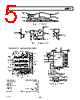


Okay, let's break down the information from this data sheet excerpt. This is a portion of an Analog Devices AD9012 data sheet. Here's a summary of the important details, organized for clarity:
1. Overview:
️· The AD9012 is a device, likely an analog-to-digital converter (ADC), used in data acquisition systems. It appears to have a resolution of 8 bits (8 data output lines: D1 - D8).
️· It features several voltage supplies (+VS, -VS, +VREF, -VREF, Analog Ground, Digital Ground).
️· The device includes analog and digital input/output pins, along with control and status signals (ENCODE, OVERFLOW, OVERFLOW INHIBIT, Hysteresis).
2. Pin Functions (Key Details):
This table describes the function of each pin on the AD9012. Here's a selection of the most significant:
️· Hysteresis: This pin controls the comparator hysteresis within the ADC. Adjusting this voltage changes the sensitivity.
️· +VREF & -VREF: These are critical reference voltage inputs. They define the positive and negative voltage range that the ADC will convert.
️· ANALOG INPUT: Analog input pins that should be connected together.
️· ANALOG GROUND: Analog ground pins that must be connected together.
️· ENCODE: A TTL-level input that initiates a conversion cycle. It's sensitive to rising edges.
️· DIGITAL +VS & -VS: These are the primary digital power supply pins (nominally +5.0 V and -5.2 V, respectively).
️· D1-D8: These are the digital output lines, representing the converted analog value (LSB to MSB).
️· OVERFLOW: A status output indicating an overrange condition (input voltage beyond the reference range). It can be enabled or inhibited (see OVERFLOW INHIBIT).
️· OVERFLOW INHIBIT: This pin controls whether the OVERFLOW output is active (enabled) or inactive (inhibited).
3. Key Operational Details:
️· Analog Input: The AD9012 converts an analog voltage into a digital word. It's crucial that the analog input voltage remains within the range defined by +VREF and -VREF.
️· Conversion Initiation: A rising edge on the ENCODE pin triggers the conversion process.
️· Overflow Condition: If the input voltage exceeds the defined reference range (+VREF or -VREF), the OVERFLOW output will assert (if OVERFLOW INHIBIT is not grounded).
️· Output Data: The digital output data (D1-D8) represents the converted analog voltage. D1 is the least significant bit (LSB), and D8 is the most significant bit (MSB).
4. Precautions and Considerations:
️· ESD Sensitivity: The device is sensitive to electrostatic discharge. Proper handling procedures are required to prevent damage.
️· Grounding: All ground pins (Analog Ground, Digital Ground) *must* be properly connected to a common ground plane.
️· Reference Voltages: The accuracy of the converted digital value depends on the stability and accuracy of the +VREF and -VREF reference voltages.
️· Power Supplies: Voltage supplies must be stable and within specified tolerances.
Let me know if you'd like a more detailed explanation of any specific aspect. For example, if you want to understand how the OVERFLOW functionality works in more detail, just ask!
1. Overview:
️· The AD9012 is a device, likely an analog-to-digital converter (ADC), used in data acquisition systems. It appears to have a resolution of 8 bits (8 data output lines: D1 - D8).
️· It features several voltage supplies (+VS, -VS, +VREF, -VREF, Analog Ground, Digital Ground).
️· The device includes analog and digital input/output pins, along with control and status signals (ENCODE, OVERFLOW, OVERFLOW INHIBIT, Hysteresis).
2. Pin Functions (Key Details):
This table describes the function of each pin on the AD9012. Here's a selection of the most significant:
️· Hysteresis: This pin controls the comparator hysteresis within the ADC. Adjusting this voltage changes the sensitivity.
️· +VREF & -VREF: These are critical reference voltage inputs. They define the positive and negative voltage range that the ADC will convert.
️· ANALOG INPUT: Analog input pins that should be connected together.
️· ANALOG GROUND: Analog ground pins that must be connected together.
️· ENCODE: A TTL-level input that initiates a conversion cycle. It's sensitive to rising edges.
️· DIGITAL +VS & -VS: These are the primary digital power supply pins (nominally +5.0 V and -5.2 V, respectively).
️· D1-D8: These are the digital output lines, representing the converted analog value (LSB to MSB).
️· OVERFLOW: A status output indicating an overrange condition (input voltage beyond the reference range). It can be enabled or inhibited (see OVERFLOW INHIBIT).
️· OVERFLOW INHIBIT: This pin controls whether the OVERFLOW output is active (enabled) or inactive (inhibited).
3. Key Operational Details:
️· Analog Input: The AD9012 converts an analog voltage into a digital word. It's crucial that the analog input voltage remains within the range defined by +VREF and -VREF.
️· Conversion Initiation: A rising edge on the ENCODE pin triggers the conversion process.
️· Overflow Condition: If the input voltage exceeds the defined reference range (+VREF or -VREF), the OVERFLOW output will assert (if OVERFLOW INHIBIT is not grounded).
️· Output Data: The digital output data (D1-D8) represents the converted analog voltage. D1 is the least significant bit (LSB), and D8 is the most significant bit (MSB).
4. Precautions and Considerations:
️· ESD Sensitivity: The device is sensitive to electrostatic discharge. Proper handling procedures are required to prevent damage.
️· Grounding: All ground pins (Analog Ground, Digital Ground) *must* be properly connected to a common ground plane.
️· Reference Voltages: The accuracy of the converted digital value depends on the stability and accuracy of the +VREF and -VREF reference voltages.
️· Power Supplies: Voltage supplies must be stable and within specified tolerances.
| Part No. | AD9012TQ |
| Manufacturer | AD |
| Size | 141 Kbytes |
| Pages | 8 pages |
| Description | High Speed 8-Bit TTL A/D Converter |
| ALLDATASHEET é útil para você? [ DONATE ] |
Sobre Alldatasheet | Publicidade | Contato conosco | Privacy Policy | Link para a ficha técnica | roca de Link | Lista de Fabricantes All Rights Reserved©Alldatasheet.com |
| Russian : Alldatasheetru.com | Korean : Alldatasheet.co.kr | Spanish : Alldatasheet.es | French : Alldatasheet.fr | Italian : Alldatasheetit.com Portuguese : Alldatasheetpt.com | Polish : Alldatasheet.pl | Vietnamese : Alldatasheet.vn Indian : Alldatasheet.in | Mexican : Alldatasheet.com.mx | British : Alldatasheet.co.uk | New Zealand : Alldatasheet.co.nz |
|
Family Site : ic2ic.com |
icmetro.com |
 Portuguese ▼
  English
 Chinese
 German
 Japanese
 Russian
 Korean
 Spanish
 French
 Italian
 Polish
 Vietnamese
 Indian
 Mexican
 British
 New Zealand