 |
Os motores de busca de Datasheet de Componentes eletrônicos |
|
|
Os motores de busca de Datasheet de Componentes eletrônicos |
|
The question interval is too short.
Please try again in a few seconds.

Hello, Please ask a question about SPT7937 Datasheet
# Example questions:
➢ What is this requirement and why is it important?
➢ What is the typical input capacitance and input resistance of the analog inputs of the spt7937, and why are these characteristics important?
➢ What are the key benefits of the auto-calibration scheme used in the spt7937?
| Part No. | SPT7937 |
| Manufacturer | CADEKA |
| Size | 177 Kbytes |
| Pages | 11 pages |
| Description | 12-BIT, 28 MSPS, 170 mW A/D CONVERTER |






1. Overview & Architecture
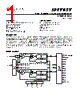
️· What is it? The SPT7937 is a CMOS Analog-to-Digital Converter (ADC).
️· High-Speed: Achieves its high sample rate by using multiple (18) SAR (Successive Approximation Register) ADC sections operating in parallel.
️· Clocking: Uses an 18-phase clock, with each ADC section sampling the input signal in sequence. The latency from analog input sample to digital output is 14 clock cycles.
️· Calibration: Uses a user-transparent, auto-calibration scheme to maintain accuracy over time and temperature.
2. Power Supplies & Grounding
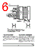
️· Configuration: Suggests using a single analog supply and a separate digital supply (for the digital output driver and interface circuitry) to prevent potential latch-up.
️· Power-up Sequence: Power supplies *must* be powered up *before* applying the analog input signal.
️· Grounding: AGND (0.0 V) is a common ground, but can be run up to 2.0 V with a second reference.
3. Voltage Reference
️· External Requirement: Needs a single external voltage reference.
️· Range: Reference voltage should be between 3V and 5V.
️· Full-Scale Range: The voltage difference between the ladder sense lines (V RHS – V RLS) should ideally be between 3V and 5V for optimal performance.
️· Simplified Configuration (Optional): Can tie V Ref directly to V RHF and AGND to V RLF, but this introduces voltage drops that need to be considered.
4. Analog Input
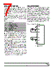
️· Range: Input voltage range is from V RLS to V RHS (typically 4.0V).
️· Minimal Drive Requirements: Very low input capacitance (5pF) and high resistance (35kΩ) reduce drive requirements.
️· Protection: Requires a series resistor and diode clamping circuit for input protection.
5. Calibration Details
️· Auto-Calibration: Continually adjusts gain and offset errors.
️· Calibration Time: Requires a minimum of 10,000 clock cycles (approx. 357 µsec at 28 MHz) to initially calibrate.
️· Continuous Operation: Clock must be continuously applied for the device to remain calibrated.
6. Table II: Clock Cycles (Highlights)
️· Clock 1: Reference Zero Sampling
️· Clock 2: Auto-Zero Comparison
️· Clock 3: Auto-Calibrate Comparison
️· Clock 4: Input Sample
️· Clock 35-47: 13-bit SAR Conversion (across 13 steps)
️· Clock 48: Data Transfer
Key Takeaways / Considerations for Use:
️· Power-Up Sequence is Critical: Get the power supply sequence right.
️· Reference Voltage: Choose a suitable reference voltage within the specified range and consider the force/sense circuit implications.
️· Input Protection: Use the recommended input protection circuit.
️· Calibration Time: Account for the initial calibration time at power-up.
️· Continuous Clock: Ensure a continuous clock signal to maintain calibration.
1. Overview & Architecture
️· What is it? The SPT7937 is a CMOS Analog-to-Digital Converter (ADC).
️· High-Speed: Achieves its high sample rate by using multiple (18) SAR (Successive Approximation Register) ADC sections operating in parallel.
️· Clocking: Uses an 18-phase clock, with each ADC section sampling the input signal in sequence. The latency from analog input sample to digital output is 14 clock cycles.
️· Calibration: Uses a user-transparent, auto-calibration scheme to maintain accuracy over time and temperature.
2. Power Supplies & Grounding
️· Configuration: Suggests using a single analog supply and a separate digital supply (for the digital output driver and interface circuitry) to prevent potential latch-up.
️· Power-up Sequence: Power supplies *must* be powered up *before* applying the analog input signal.
️· Grounding: AGND (0.0 V) is a common ground, but can be run up to 2.0 V with a second reference.
3. Voltage Reference
️· External Requirement: Needs a single external voltage reference.
️· Range: Reference voltage should be between 3V and 5V.
️· Full-Scale Range: The voltage difference between the ladder sense lines (V RHS – V RLS) should ideally be between 3V and 5V for optimal performance.
️· Simplified Configuration (Optional): Can tie V Ref directly to V RHF and AGND to V RLF, but this introduces voltage drops that need to be considered.
4. Analog Input
️· Range: Input voltage range is from V RLS to V RHS (typically 4.0V).
️· Minimal Drive Requirements: Very low input capacitance (5pF) and high resistance (35kΩ) reduce drive requirements.
️· Protection: Requires a series resistor and diode clamping circuit for input protection.
5. Calibration Details
️· Auto-Calibration: Continually adjusts gain and offset errors.
️· Calibration Time: Requires a minimum of 10,000 clock cycles (approx. 357 µsec at 28 MHz) to initially calibrate.
️· Continuous Operation: Clock must be continuously applied for the device to remain calibrated.
6. Table II: Clock Cycles (Highlights)
️· Clock 1: Reference Zero Sampling
️· Clock 2: Auto-Zero Comparison
️· Clock 3: Auto-Calibrate Comparison
️· Clock 4: Input Sample
️· Clock 35-47: 13-bit SAR Conversion (across 13 steps)
️· Clock 48: Data Transfer
Key Takeaways / Considerations for Use:
️· Power-Up Sequence is Critical: Get the power supply sequence right.
️· Reference Voltage: Choose a suitable reference voltage within the specified range and consider the force/sense circuit implications.
️· Input Protection: Use the recommended input protection circuit.
️· Calibration Time: Account for the initial calibration time at power-up.
️· Continuous Clock: Ensure a continuous clock signal to maintain calibration.
| Part No. | SPT7937 |
| Manufacturer | CADEKA |
| Size | 177 Kbytes |
| Pages | 11 pages |
| Description | 12-BIT, 28 MSPS, 170 mW A/D CONVERTER |
| ALLDATASHEET é útil para você? [ DONATE ] |
Sobre Alldatasheet | Publicidade | Contato conosco | Privacy Policy | Link para a ficha técnica | roca de Link | Lista de Fabricantes All Rights Reserved©Alldatasheet.com |
| Russian : Alldatasheetru.com | Korean : Alldatasheet.co.kr | Spanish : Alldatasheet.es | French : Alldatasheet.fr | Italian : Alldatasheetit.com Portuguese : Alldatasheetpt.com | Polish : Alldatasheet.pl | Vietnamese : Alldatasheet.vn Indian : Alldatasheet.in | Mexican : Alldatasheet.com.mx | British : Alldatasheet.co.uk | New Zealand : Alldatasheet.co.nz |
|
Family Site : ic2ic.com |
icmetro.com |
 Portuguese ▼
  English
 Chinese
 German
 Japanese
 Russian
 Korean
 Spanish
 French
 Italian
 Polish
 Vietnamese
 Indian
 Mexican
 British
 New Zealand