 |
Os motores de busca de Datasheet de Componentes eletrônicos |
|
|
Os motores de busca de Datasheet de Componentes eletrônicos |
|
The question interval is too short.
Please try again in a few seconds.

Hello, Please ask a question about ADP2450ACPZ-2-R7 Datasheet
# Example questions:
➢ What safety features are indicated in the block diagram, and how do they contribute to the overall system reliability?
➢ The diagram shows multiple output stages (eout1-4) connected to programmable gain amplifiers. what is the potential purpose of these amplifiers and output stages in a system context?
➢ What are the primary power sources utilized by the adp5090/1/2?
| Part No. | ADP2450ACPZ-2-R7 |
| Manufacturer | AD |
| Size | 984 Kbytes |
| Pages | 40 pages |
| Description | Power Management IC for Circuit Breaker Applications |

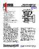













Overall Purpose:
The ADP5563 is a complex power management IC designed to handle multiple voltage rails, with features including boost, buck, and actuator control, along with protection and monitoring.
Key Blocks & Functions (Based on the Diagram):
1. Boost Shunt Controller:
- Used for regulating a voltage using a boost topology.
- Includes UVLO (Under Voltage Lockout) functionality.
- Incorporates reset generation.
2. Buck Regulator:
- A standard buck regulator for voltage conversion.
- Includes TSD (Thermal Shutdown) protection.
3. Actuator Driver:
- Provides control for an actuator.
4. Power Detection & Reset Generator:
- Monitors power status and generates reset signals.
5. Gain Setting PGAs (Programmable Gain Amplifiers):
- Multiple PGAs (PGA1-PGA4) are present, allowing for adjustable gain in signal processing or sensing.
6. Comparator (CMP) and Slope Compensation/Ramp Generator:
- Used in control loops to compare voltage levels and to smooth out signal transitions.
7. Low-Side Current Sense:
- Used to measure current for overcurrent protection and other monitoring functions.
8. Control Logic:
- Centralized logic block coordinating all the IC's functions.
9. Multiple Voltage Rails:
- The IC appears to handle multiple voltage rails, with references to 8V, 5V, and other voltage levels.
10. Output Stages (EOUT1-EOUT4):
- The various output rails from the internal circuits.
Key Features Highlighted:
️· Comprehensive Protection: Includes UVLO, TSD, and overcurrent protection.
️· Programmability: The PGAs offer programmable gain for flexibility.
️· Multiple Voltage Regulation: Capable of regulating various voltage rails.
️· Integrated Control: Centralized control logic to coordinate all functionalities.
Note: This is based purely on interpreting the visual block diagram. A full understanding would require the ADP5563 datasheet, which would explain the operation of each block in detail.
Overall Purpose:
The ADP5563 is a complex power management IC designed to handle multiple voltage rails, with features including boost, buck, and actuator control, along with protection and monitoring.
Key Blocks & Functions (Based on the Diagram):
1. Boost Shunt Controller:
- Used for regulating a voltage using a boost topology.
- Includes UVLO (Under Voltage Lockout) functionality.
- Incorporates reset generation.
2. Buck Regulator:
- A standard buck regulator for voltage conversion.
- Includes TSD (Thermal Shutdown) protection.
3. Actuator Driver:
- Provides control for an actuator.
4. Power Detection & Reset Generator:
- Monitors power status and generates reset signals.
5. Gain Setting PGAs (Programmable Gain Amplifiers):
- Multiple PGAs (PGA1-PGA4) are present, allowing for adjustable gain in signal processing or sensing.
6. Comparator (CMP) and Slope Compensation/Ramp Generator:
- Used in control loops to compare voltage levels and to smooth out signal transitions.
7. Low-Side Current Sense:
- Used to measure current for overcurrent protection and other monitoring functions.
8. Control Logic:
- Centralized logic block coordinating all the IC's functions.
9. Multiple Voltage Rails:
- The IC appears to handle multiple voltage rails, with references to 8V, 5V, and other voltage levels.
10. Output Stages (EOUT1-EOUT4):
- The various output rails from the internal circuits.
Key Features Highlighted:
️· Comprehensive Protection: Includes UVLO, TSD, and overcurrent protection.
️· Programmability: The PGAs offer programmable gain for flexibility.
️· Multiple Voltage Regulation: Capable of regulating various voltage rails.
️· Integrated Control: Centralized control logic to coordinate all functionalities.
Note: This is based purely on interpreting the visual block diagram. A full understanding would require the ADP5563 datasheet, which would explain the operation of each block in detail.
| Part No. | ADP2450ACPZ-2-R7 |
| Manufacturer | AD |
| Size | 984 Kbytes |
| Pages | 40 pages |
| Description | Power Management IC for Circuit Breaker Applications |
| ALLDATASHEET é útil para você? [ DONATE ] |
Sobre Alldatasheet | Publicidade | Contato conosco | Privacy Policy | Link para a ficha técnica | roca de Link | Lista de Fabricantes All Rights Reserved©Alldatasheet.com |
| Russian : Alldatasheetru.com | Korean : Alldatasheet.co.kr | Spanish : Alldatasheet.es | French : Alldatasheet.fr | Italian : Alldatasheetit.com Portuguese : Alldatasheetpt.com | Polish : Alldatasheet.pl | Vietnamese : Alldatasheet.vn Indian : Alldatasheet.in | Mexican : Alldatasheet.com.mx | British : Alldatasheet.co.uk | New Zealand : Alldatasheet.co.nz |
|
Family Site : ic2ic.com |
icmetro.com |
 Portuguese ▼
  English
 Chinese
 German
 Japanese
 Russian
 Korean
 Spanish
 French
 Italian
 Polish
 Vietnamese
 Indian
 Mexican
 British
 New Zealand